Minimum order value ₹99.00 · Get 10% Off on Cart Value use Coupon code VASP10 · Free shipping over ₹999.00

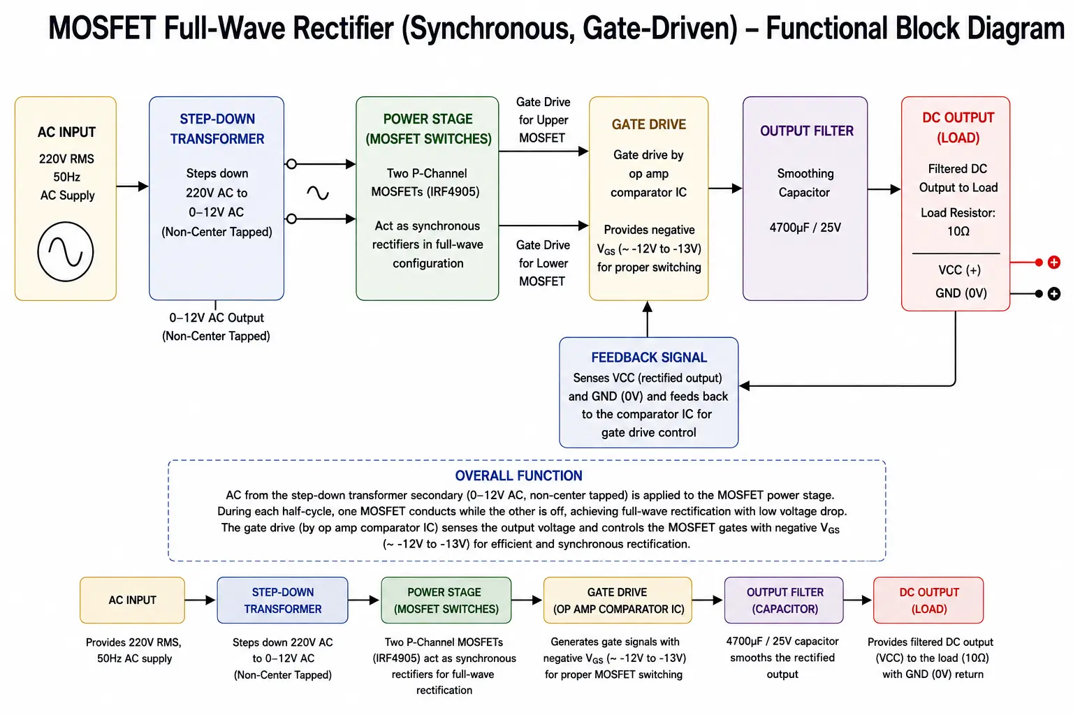
Using MOSFETs as Rectifiers to Make Ideal diode – an Experimental Project

A conventional bridge rectifier is simple, reliable and inexpensive, but it has one unavoidable disadvantage: the current passes through semiconductor junctions that introduce a forward-voltage drop. At higher currents, that voltage drop becomes significant and the resulting power loss can become substantial.
A MOSFET-based ideal-diode full-wave rectifier takes a different approach. Instead of relying on the forward drop of ordinary diodes, MOSFETs are actively controlled so that they conduct only when the polarity is correct. When the MOSFET is fully open to current, its resistance can be very low, making the voltage drop potentially only a few millivolts to a few hundred millivolts depending on the MOSFET and load current.
This makes the technique particularly interesting for low-voltage, high-current power supplies.
What Is a MOSFET Ideal-Diode Rectifier?
A MOSFET ideal-diode rectifier is essentially a synchronous rectifier with active polarity control.
Instead of:
AC → diode bridge → filter capacitor → DC
the basic idea is:
AC → MOSFET rectification stage → filter capacitor → DC
The MOSFETs are controlled by a comparator or control circuit that detects the instantaneous polarity of the AC waveform.
When the correct half-cycle arrives, the appropriate MOSFETs are turned ON. During the opposite half-cycle, they are turned OFF and the other pair conducts.
The result is full-wave rectification while avoiding the relatively large forward voltage associated with conventional silicon diodes.
How It Works — Step by Step
1. AC Enters the Rectifier
The AC source is normally supplied by a step-down transformer.
For example, a transformer secondary may provide 12 V AC.
The secondary produces a waveform that continuously changes polarity:
Positive half-cycle → zero → negative half-cycle → zero
The MOSFET control circuit determines which polarity is present.
2. The MOSFETs Replace the Conventional Rectifier Diodes
A conventional bridge uses four diodes.
Each half-cycle turns on two diodes and blocks the other two.
In the MOSFET version, MOSFETs perform the same basic switching function, but their conduction is controlled electronically.
When a MOSFET is turned fully ON, the important parameter becomes its RDS(on) rather than a diode’s fixed forward voltage.
For example, if a MOSFET has:
RDS(on) = 10 mΩ
and the rectifier is carrying:
10 A
the approximate MOSFET conduction drop is only:
0.1 V
and the conduction loss is approximately:
1 W
That is very different from forcing 10 A through a conventional silicon diode with a much larger forward voltage.
3. The Control Circuit Detects the AC Polarity
The MOSFETs cannot simply be connected and left uncontrolled.
The circuit needs to determine which MOSFET pair should conduct.
This is where the comparator/gate-drive section becomes important.
The comparator monitors the relevant AC/input voltages and produces control signals according to their polarity.
4. The Correct MOSFETs Are Switched ON
During one half-cycle, the control circuit turns on the MOSFETs that provide the correct current path.
During the opposite half-cycle, that pair is turned OFF and the opposite pair is enabled.
Therefore the current through the load always has the same polarity, even though the transformer secondary current reverses every half-cycle.
This is the essential operation of a full-wave rectifier.
5. The MOSFET Channel Provides the Low-Resistance Current Path
When the MOSFET is fully open, the current path has very low resistance compared with a conventional diode.
The actual voltage drop therefore depends heavily on:
- MOSFET RDS(on)
- load current
- gate-drive voltage
- MOSFET temperature
- PCB resistance
- wiring resistance
6. The Output Capacitor Smooths the Rectified DC
After rectification, a large electrolytic capacitor can be connected across the DC output.
For example:
4700 µF
The capacitor charges from the rectified waveform and supplies current to the load between charging peaks, thereby smoothing the output DC.
Why Use MOSFETs Instead of Diodes?
The biggest attraction is low conduction loss.
Consider a conventional silicon bridge carrying 10 A.
If approximately 1 V is lost across each conducting diode and two diodes conduct at a time:
Total drop ≈ 2 V
The rectifier could therefore dissipate roughly:
20 W
That is a considerable amount of heat.
A MOSFET rectifier can potentially have a much smaller conduction loss.
For example, if the total effective resistance of the conducting MOSFET path were 20 mΩ:
10 A × 0.020 Ω = 0.20 V
The corresponding conduction loss would be:
10² × 0.020 = 2 W
The exact result depends on the actual MOSFETs and circuit, but this illustrates why active rectification becomes attractive at high current.
Main Benefits
1. Very Low Forward Voltage Drop
This is the biggest advantage.
A properly driven MOSFET can have a voltage drop far below that of a conventional silicon rectifier diode.
For low-voltage supplies, this can make a substantial difference.
2. Higher Efficiency
Lower voltage drop means lower conduction loss.
Less power is converted into heat inside the rectifier.
This can improve overall power-supply efficiency.
3. Lower Heat Generation
Because the rectifier dissipates less power, the heatsink requirement can potentially be reduced.
This is particularly valuable when the output current is high.
4. Particularly Useful at Low Voltage
The advantages become increasingly important as the supply voltage decreases.
For example, losing 1–2 V in a rectifier is a much bigger percentage of a 12 V supply than of a 230 V supply.
Therefore MOSFET rectification is especially attractive for:
- 5 V supplies
- 9 V supplies
- 12 V supplies
- high-current battery chargers
- low-voltage SMPS systems
- high-current DC power supplies
5. Full-Wave Operation
Both halves of the AC waveform are utilized.
This provides the same fundamental full-wave advantage as a conventional bridge.
The Drawbacks
The MOSFET approach is not automatically better than a diode bridge.
Its biggest disadvantage is complexity.
1. Gate-Drive Circuit Is Required
A diode automatically conducts when forward biased.
A MOSFET does not automatically behave like an ideal diode simply because it is present in the circuit.
The gate must be driven correctly.
The control circuit must determine:
- when to turn the MOSFET ON
- when to turn it OFF
- which MOSFET pair should conduct
This makes the design considerably more complicated.
2. Incorrect Timing Can Cause Problems
The gate-drive timing is critical.
If MOSFETs that should be OFF remain ON at the wrong time, they can provide an unwanted current path.
In a badly designed circuit, this can result in:
- excessive current
- cross-conduction
- transformer loading
- MOSFET heating
- distorted output
- MOSFET failure
Therefore the control circuit needs adequate attention to switching thresholds and timing.
3. MOSFET Body Diodes Still Exist
A MOSFET is not a diode-free device.
Every power MOSFET contains an intrinsic body diode.
If the MOSFET is not driven correctly, current may still flow through that diode.
Therefore the circuit must be designed so that the MOSFET channel conducts whenever possible and the body diode does not become the primary rectification path.
4. Gate Voltage Must Be Correct
The MOSFET must receive sufficient gate-source voltage to achieve low RDS(on).
This is particularly important when using different MOSFET types.
The designer must consider:
VGS, not simply the gate voltage relative to ground.
This becomes especially important when the MOSFET source is moving with the AC waveform or output voltage.
5. Comparator Limitations
Using a comparator for the gate-control function is practical, but it is not automatically a dedicated high-speed MOSFET gate driver.
The designer needs to consider:
- comparator propagation delay
- output transistor characteristics
- gate charging current
- MOSFET gate capacitance
- switching speed
- pull-up resistor values
- noise around the zero crossing
At 50 Hz, the frequency itself is not demanding, but the transition around each zero crossing still matters.
6. MOSFET Selection Is Important
The lowest RDS(on) MOSFET is not automatically the best choice.
The designer must consider:
- VDS rating
- RDS(on)
- maximum current
- gate charge
- VGS rating
- thermal characteristics
- package
- body-diode characteristics
- safe operating area
A MOSFET with very low RDS(on) may have a large gate charge, making it harder for the comparator circuit to drive directly.
What Happens Near the Zero Crossing?
This is one of the most important parts of an ideal-diode rectifier.
Near the AC zero crossing, the voltage difference between the two sides becomes very small.
The control circuit therefore has to decide when the conducting MOSFET pair should turn OFF and when the opposite pair should turn ON.
If the transition is too early or too late, unwanted current can flow.
This is why a real hardware circuit can behave differently from an ideal simulation.
The comparator, MOSFET gate charge, PCB parasitics and transformer characteristics all affect the actual transition.
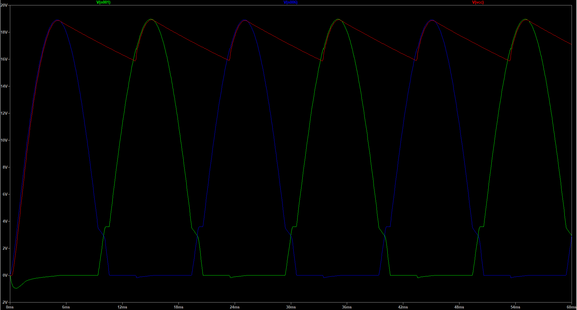
- Green / blue trace – input. Red trace – output.
Simulation vs Real Hardware
A simulation is extremely useful for developing this type of circuit, but it should not be treated as proof that the PCB will work perfectly.
A simulation can demonstrate that:
- the MOSFETs switch in the intended sequence
- the output follows the rectified waveform
- the voltage drop is very small
- the current flows through the intended MOSFETs
- the control circuit responds to the AC polarity
But the physical circuit introduces additional factors.
These include:
- transformer leakage inductance
- wiring resistance
- PCB track resistance
- MOSFET gate charge
- comparator propagation delay
- component tolerances
- temperature
- switching transients
- electrical noise
Therefore the final PCB should be tested progressively rather than immediately applying the maximum expected load.
MOSFET Rectifier vs Conventional Bridge
| Feature | Conventional Diode Bridge | MOSFET Ideal-Diode Rectifier |
|---|---|---|
| Circuit complexity | Very low | Higher |
| Voltage drop | Relatively high | Potentially very low |
| Conduction loss | Higher | Lower |
| Heat generation | Higher | Lower |
| Gate-drive circuit | Not required | Required |
| Control circuit | Not required | Required |
| Component cost | Low | Higher |
| Design difficulty | Easy | Moderate/High |
| High-current operation | Possible | Very attractive |
| Low-voltage operation | Less efficient | Particularly attractive |
| Failure/debugging | Simple | More complicated |
Is It Really an “Ideal Diode”?
Not literally.
The term ideal diode describes the desired behavior rather than a perfect physical device.
A real MOSFET rectifier still has:
- RDS(on)
- switching losses
- body-diode behavior
- gate-drive losses
- PCB resistance
- control delays
So the voltage drop is not actually zero.
However, compared with a conventional diode, the drop can be sufficiently small that the circuit behaves much more like an ideal diode.
Where This Design Makes the Most Sense
A MOSFET full-wave rectifier is most attractive when current is high and voltage is relatively low.
For a small low-current power supply, a conventional bridge may be the better engineering choice because it is cheap, simple and extremely reliable.
But when the rectifier is handling substantial current, reducing the rectifier voltage drop can save a significant amount of power.
That is where the extra complexity of active MOSFET rectification starts to make sense.
Final Verdict
A MOSFET-based ideal-diode full-wave rectifier is an excellent example of replacing a simple but lossy passive component with an actively controlled semiconductor switch.
Its fundamental advantage is straightforward:
A diode uses its forward voltage; a MOSFET can use its very low ON resistance.
The result can be:
- substantially lower voltage drop
- lower conduction losses
- less heat
- improved efficiency
- particularly good performance in low-voltage/high-current applications
The price is complexity. The MOSFETs need proper gate control, the comparator circuit must switch the correct devices at the correct time, and the PCB must be designed with the resulting currents and transients in mind.
So the MOSFET ideal-diode rectifier is not a universal replacement for a diode bridge. It is a specialized solution where the reduction in conduction loss justifies the additional circuitry.
For a properly designed 50 Hz, low-voltage, high-current transformer supply, however, it can be a very worthwhile approach.
PS
PS: We’re currently developing a dedicated PCB for this MOSFET ideal-diode full-wave rectifier. Both blank PCBs for DIY builds and fully assembled, ready-to-use boards will be available on our website soon. We’ll be posting detailed pictures of the PCB and assembled version shortly, along with specifications and availability.


